


13.8V 20A power supply
Regulated DC power supply, short circuit safe, and with current limiter
This PSU has been especially designed for current-hungry ham radio transceivers. It delivers safely around 20Amps at 13.8V. For lower currents, a separate current limiting output, capable of 15ma up to a total of 20A has been added. Let us see what we have got here. The power transformer should be capable to deliver at least 25A at 17.5 to 20V. The lower the voltage, the lower power dissipation. The rectified current will be “ironed” by the C1, whose capacity should not be less than 40.000uF, (a golden rule of around 2000uF/A), but we recommend up to 50.000uF. This capacity can be built up by several smaller capacitors in parallel. The base of this design is a simple 12V regulator (7812). The output voltage can be brought to desired value (here 13.8V) by two external resistors (R5 and R6) using this formula:
U= 12(1+R5/R6)
The low currents (here 15mA) will keep the 7812 in its regular function. As soon as the current rises over 15ma, the voltage drop on R4 will “open” the Q3, actually handling the high output current. This is a PNP transistor (Ic>25) and current amplification factor of at least 20. The one that has been tested and proven here is the 2N5683. The current limiting resistance RL, for the maximum output of 20 Amps should be 0.03 Ohms, rated at
least 15W. You can use the resistance wire or switch several resistors in parallel, totaling the resistance/power values. Values for other currents can be calculated by the rule:
RL=0.7/Imax
The RL and Q2 (3A PNP such as BD330) form a short circuit “automatic fuse”. As soon as the maximum current reaches 20Amps, the voltage drop over the resistor RL will open Q2, and thus limit the B-E Current of Q3. Parallel to Q2 is Q1, which lights the LED 1 whenever the current limiting circuit is active. When the “fuse” is active, the Q2 bridges the R3, so the full current would flow through the IC1, and damage it. Therefore the R4 is inserted, as to limit the IC1 current to 15mA. This makes it possible to run the IC1 without any cooling aid. The LED 2 will light up every time the PSU is switched on.
There is an adjustable current limiter in parallel to the fixed output, thus providing adjustable current source for smaller currents.
This circuit is very simple too. You will notice that there is no current sensing resistor. But it is really there, in a form of the Rds-on resistance of the N-channel FET, which actually handles the load cutoff from the source. The function of the FET is shown in the diagram 2. When the current Id is rising, the tension Uds over the resistance Rds rises very slowly in the beginning, but very fast after the knick. This means, that before the knick the FET behaves as a resistor but after it, works as constant current source.
The D2, R3 and B-E connection of the Q4 will sense the Uds voltage of the FET1. When the voltage rises enough, the Q4 will shortcut the FET1 gate to mass, and cut the current flow through the FET 1 off. However, to enable the FET1 to open, there is certain gate voltage necessary, which in this case is brought up by the voltage divider consisting of R8, Z1, P1 and R9. So the maximum Gate voltage will be the one of the Z1, and the minimal will be around 3V6. The Z1 voltage (Uz1) will thus determine the max current flowing through the FET 1.
The diagram 2 will show that for 5 Amps the Uz1 should be 5V6, and for 20Amps around 9V6. The Capacitor C4 will determine the “velocity” or the reaction time of the limiter. 100 uF will make the reaction time to be around 100ms, and 1n will make it 1us.
Within the designed limits, the P1 will limit the current output in the range of 15mA to 20A. You can use both output simultaneously, but the total output current will be limited by the value of the RL. This PSU can be built also for higher outputs, as long as the transformer will handle the current requirements, and you provide sufficient cooling for the Q3.
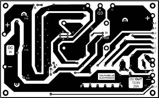
If somebody will be interested, there is a PCB design ready.
Have fun.
Bob
REV1.
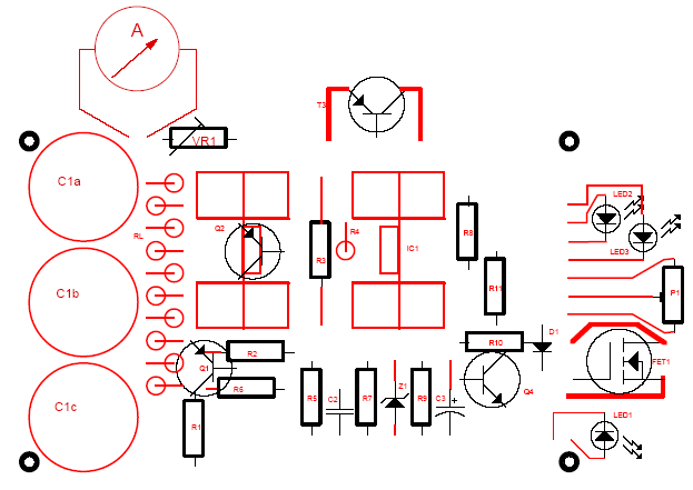
I have received several requests for some modifications, and the one I find useful is the addition of an amp meter. Therefore the slightly modified diagram is included in this revision. All elements within the dotted border are now placed on the pcb. There is also elements placement design included. Should one have an 25Amp instrument on hand, there is nothing easier. Just mount it in line and there it goes. However, a ham would probably find an instrument somewhere in his “junk-box”, but the scale would be something completely different, let say an “S” or Voltmeter. No problem. We already have a “shunt” for the amp-meter, and it is there as the Current limiting resistor “RL”. As already known from before, there is a voltage drop of 0V7 over the resistor at current flow of 20A. What we now have to do, is to simply measure the voltage drop over the resistor, and co-relate it with the current. Let us say that our instrument has an internal resistance of 13R, and has a full scale reading of 60mV. The voltage drop over the RL is 0V7 for 20Amps. Therefore, we need another resistance in line with the instrument, that would bring the 0V7 to 60mV, or an voltage drop of 640mV.
The formula is simple:
U1:R1=U2:R2
60:13=640:X
X=13x640/60
X=138.66
Therefore, the resistance that has to be inserted in line is around 140R. I suggest to insert a trimmer (VR1) of around 200R, to fine trim the reading when calibrating the instrument. Using your favorite drawing software, design your scale to your likings, (at least 20A for the full scale) and insert it in the instrument you have. Due to the many requests for the PCB Layout, I have included the design here. The exact dimensions of the pcb are 160x100mm. Please remember, that the pcb has to be printed as a mirror image, to obtain higher quality when transferring it to the copper side of the board.
Wish you a good time.
Bob


Search Site | WWW Search | Upload Center | Support us | Advertising | FAQ | Profile | Books | Gadgets | Add your link here
Free
Schematics Search Engine | Electronic Kits | Best Buy Mobile Phones
Any
logo, trademark and project represented here are property of their
respective owner